Hello,
Actually I have two questions:
1 The transistor is used as a switch (current/no current or 0 or 1). But how does a transistor know whether or not it should switch? And how does this relate to programming?
2 The transistor consists of silicon with an addition of boron and phosphorus. This gives you n or p-silicon.
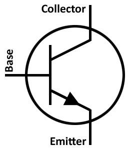
Furthermore, a transistor is a cylindrical small piece of silicon with dimensions of a few nanometers (made with the aid of a microscope). But as you can also see in the picture, it also consists of a pattern that represents base, collector and emitter.
My question is: How am I supposed to imagine that base, collector, emitter pattern? Is this burned into it using UV light or is it a pattern of a metal in the dimensions of nanometers?
I hope my questions are clear and I hope you can give me an understandable explanation,
Thanks in advance.
Sincerely.

Answer
Best,
answer to question 1:
-a transistor can be used as a switch. Usually, however, it is used in its conduction area. By sending a current into the base, a current will flow between the collector and the emitter that is Hfe (amplification factor) greater.
-when you refer to a transistor as a memory element, it is a different type. A floating gate MOSFET is used as the memory cell. A MOSFET is a transistor that is not controlled with current, but with voltage. By storing electrons in an insulated plate (floating gate), the transistor will block or conduct more easily. The presence or absence of those electrons will influence the operation of the MOSFET and thus “remember” which information (o or 1) is stored.
Answer to question 2:
Transistors are made from a “block” of silicon or germanium. By shielding certain parts of the block with a “paint”, the other parts can be contaminated with the doping material (phosphorus, …). By subjecting the block to repeated operations, different P and N regions are obtained. In an IC (integrated circuit) this can amount to millions of P and N areas. Those areas are connected with metal conductors to make the final circuit.
The paint is applied using photographic techniques (exposure, development, etching).
BEST REGARDS
Answered by
ing Marc Roggemans
microcontrollers

http://www.thomasmore.be
.