This article is about this: https://www.rt.com/news/418754-single-atom-trap-photo/

Answer
Dear Paul,
Materials scientists have several ways to “see” individual atoms. But just like with the photo you refer to, this doesn’t all work just like that. Atoms are extremely small; they have a radius of 0.5 (Hydrogen) to about 3 Ångström (Caesium). If you want to get an idea of how small this is, take an A4 and tear it in half 60 times along the shortest direction (tear and turn 90° before tearing again), you will get a sheet of about 2×3 Ångström.
To make something so small visible, you have to enlarge its image in some way. In the case of the photo you refer to, this is by allowing a very long exposure. The atom we “see” is illuminated with a blue laser. It takes in light from that which it re-emits itself. The atom does not do this in 1 specific direction but in all directions. It therefore shoots back light particles (photons) in all possible directions, which can then be captured by a light-sensitive sensor (e.g. a photographic plate or the CCD chip of a digital camera). Because the atom is so small, you can imagine that only occasionally such a photon from this atom hits the CCD of the camera. So if you want to create an image of it, you have to expose the photo for a long time. (It’s like photographing a starry sky. The longer you expose, the more stars become visible.) The final photo will then show a bright spot on 1 or a few adjacent pixels.
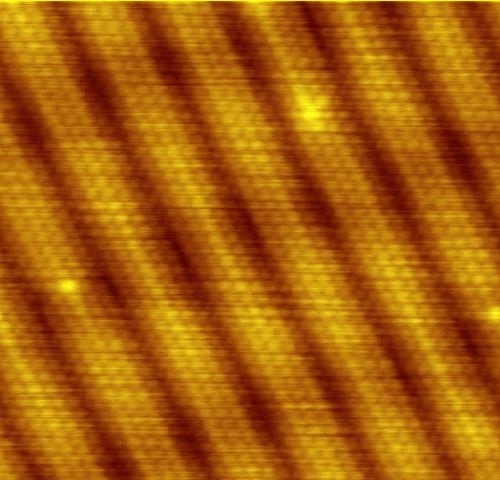
However, this is not the first time individual atoms have been made visible. Modern materials research constantly uses techniques that can make individual atoms visible. The first is the STM: the scanning tunnel microscope. This involves moving a very sharp needle over the surface of a material in order to map the mountains and valleys on that surface. This can be done with such precision that individual atoms become visible as hills. A second technique is TEM: transmission electron microscopy. A beam of electrons is shone through a material. The atoms then become visible as the places where no electrons passed through the material. This is a common way to check crystal lattices and see how different materials transition into each other when they are layered on top of each other.
Regards,
Danny

Answered by
Dr. Danny Vanpoucke
Computational materials research

Agoralaan University Campus Building D BE-3590 Diepenbeek
http://www.uhasselt.be/
.