")
In the previous edition of PC-Active you can read the first part about designing printed circuit plates with libreppcb. In this second part we will discuss the creation of our own parts.
Erik crooked
![]()
In PC-Active 338 you can read the workshop on the self-designing printing plates (PCBs) with the help of Libreppcb. Unfortunately, standard libraries in Libreppcb are still far from complete. The symbols of some electrical components are available, but the footprint not. This is the case for transistors, for example. Footprints are available from other parts, but no symbols. With the developers, there is a desire to supplement this, but that still takes the necessary time. Fortunately, it is not too difficult to draw missing parts itself. If you want to place a rectifier at the plate with the LED that we have already made, you are unlucky. Both the symbol and the footprint are missing for rectifiers. They must therefore both be made themselves.
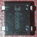 |
| Rectifier |
Go to the Library Manager. Here we have a new (local) library. In the right half we go to the tab Create Local Library. The important fields have already been filled with example settings and text in gray. If desired, you can change it by entering your own desired values. Click on Create Library. Your new library is directly on the left in the list.
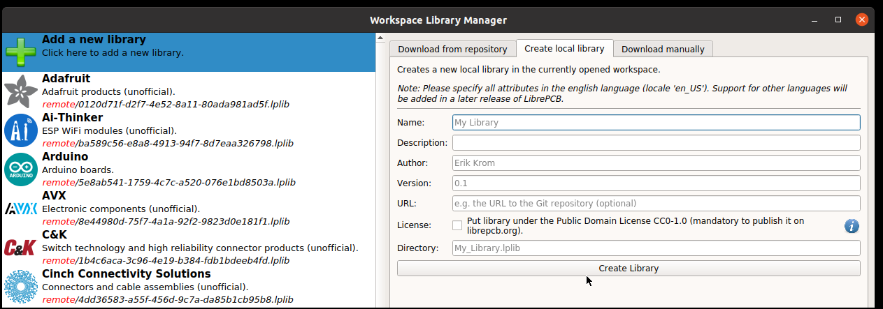 |
| Create your own library in the Library Manager |
Open the library by clicking double or with the button Open Library Editor. Now we get a screen with six empty fields. This includes the lists with different elements of our own electrical components. The symbol comes in the top row. In the bottom row there is everything that concerns the footprint and the complete part. To make a new element, we click on New Library Element In the toolbar at the top left.
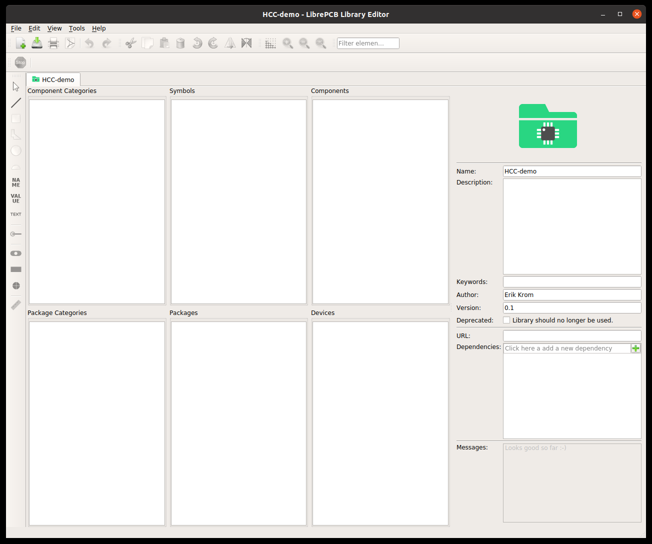 |
| Libary Editor of Libreppcb |
Category
The right categories are already available for most common components, but if you are going to make a part for which there is not yet, you can of course make your own (sub) category.
Symbol
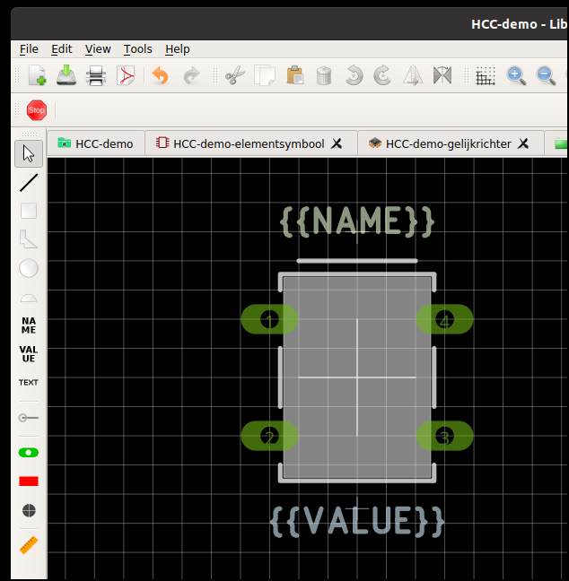
Making a component is needed a symbol. If it does not yet exist, you have to deal with it yourself. When creating a new element, choose Symbol. Give a name. Keywords are useful to indicate with which search terms this part may be found if a search field is used. At the bottom of Category the category can be chosen where the symbol would belong.
Now the symbol can be signed. The rectifier symbol can be drawn with the line and figure tools in the left toolbar. The Line,, ” Square,, ” Polygon and semicircle are basically the same. They are all a series of two or more points with a line in between. The curvature of the line is set by setting a corner. The circle is different from the other forms. This has a center and a diameter.
There are no connections with the drawing of the lines. These must be defined separately. In the tools toolbar Click on the Add Pin-button with a horizontal line starting with a green circle.
When signing a chip or something, the connections are only drawn left and right. Not above or below. The numbering starts at the top left in general runs left from top to bottom and then to the right from the bottom to top.
Finally, we add the fields for the Name and Value.
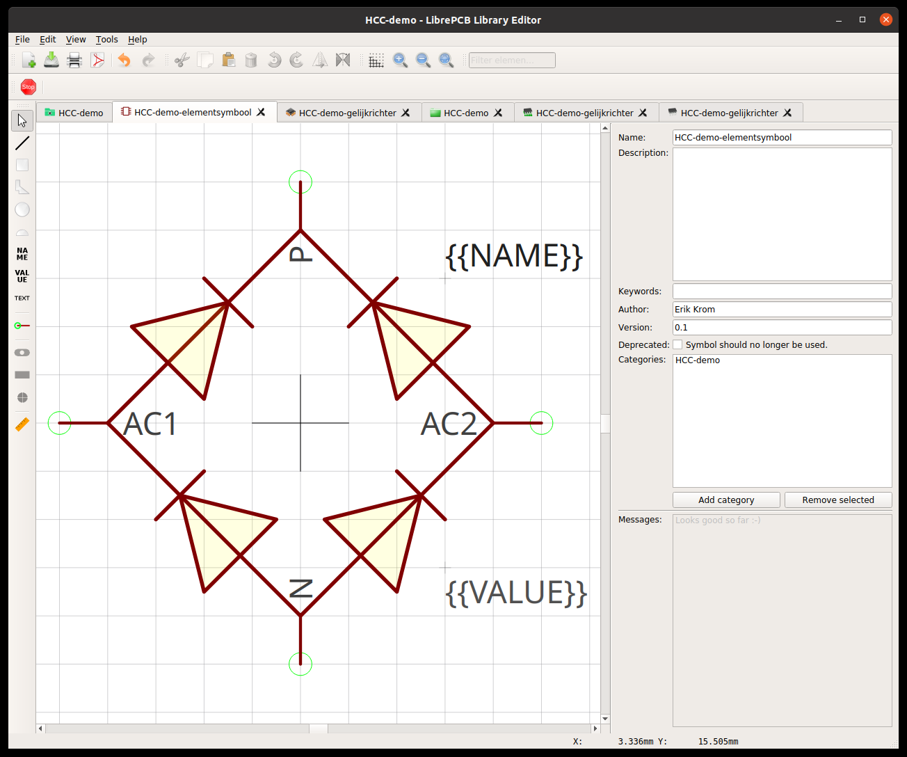 |
| Symbol of a component |
For everything, for the placement, part of the properties can be determined in advance in a toolbar at the top of the window. After installation, the properties can still be adjusted by double -clicking or right -clicking and then Property. There will be a separate window with the properties. There are often more settings here than in the toolbar at the top.
Component
If the necessary symbol is available, defining the component can be started. When creating a new element, choose Component. Again we are asked about name, description, etc. Just like when creating the symbol. This is because multiple components can use the same symbol or a component can be made up of multiple symbols.
 |
| Component Features |
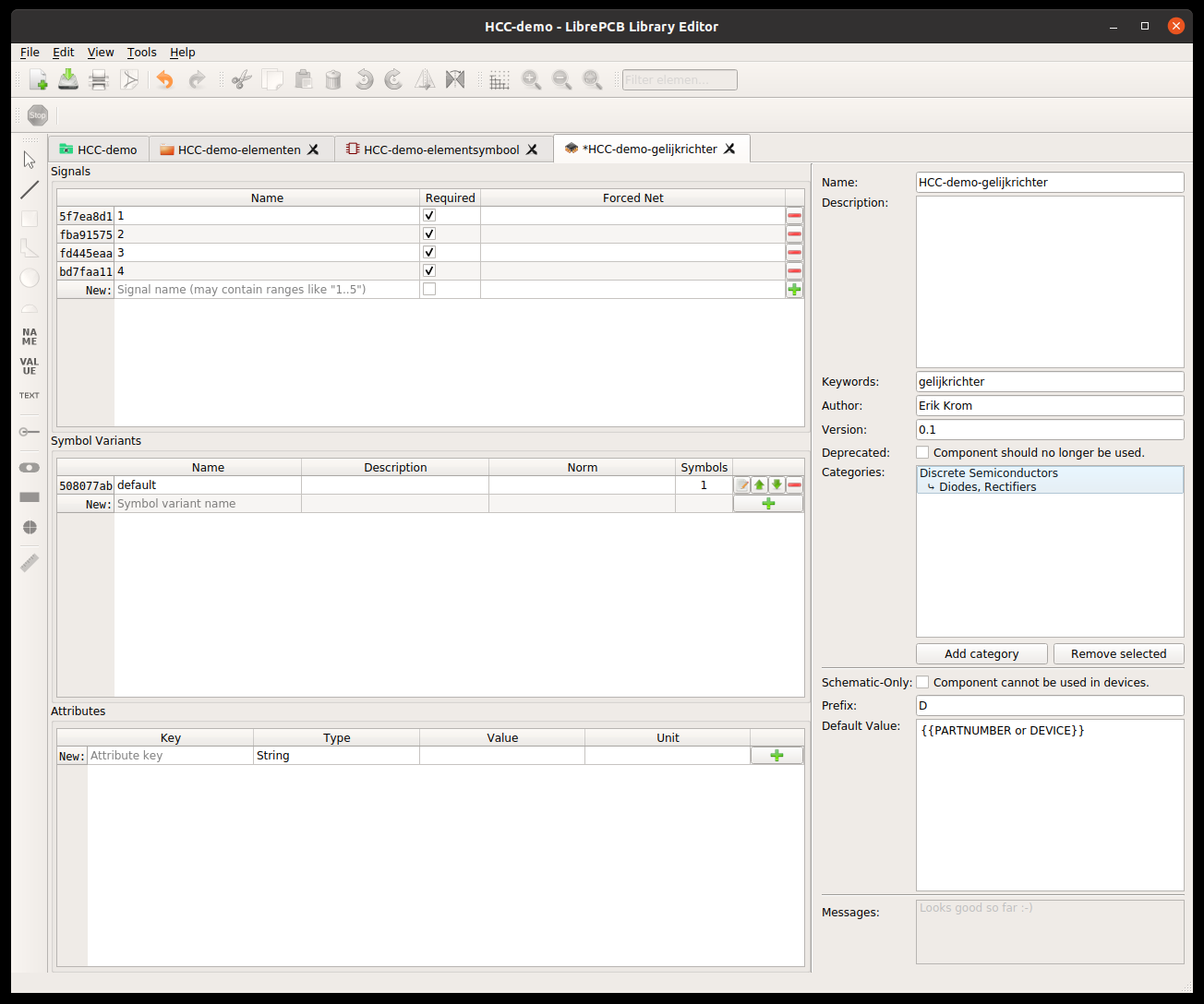
After this are in a number of steps, as in one wizardto fill in the remaining properties. Prefix Is the text that at the start of the name-Veld. When placing the components in an electric schedule, Libreppcb puts a number behind it itself, starting with 1. Suppose you fill in Prefix A In, when placing this component in the schedule, the first component A1, the second A2 and so on will be called. Many types of electrical parts have standard Prefixes: have resistances R, capacitors C, diodes D, transistors Q, chips IC, and so on.
Bee Default Value can be filled in what’s in it Value-Veld must come. A word in capital letters between double batteries or braces {{}} is seen as a variable. This can be set later in the properties of the part while making a circuit.
After this, it must be indicated which symbol must be used. Select the desired symbol and add it to the list of the green + at the end. If desired, more symbols can be added. This applies to, for example, a relay where the coil (s) and switch (s) can be put together separately. Subsequently, the connection pins will continue. The connections drawn in the symbol are automatically included in the list. The pins that must be connected can be checked under Required. This ensures that the report comes if they have forgotten when making an electric schedule. Finally, the names of the connections can be defined. These are usually the same as the connections in the symbol. Button Automatically Assign All Signals by Name the names of the symbol are taken over. After Finish The component is ready and can be used in a circuit. Afterwards, all settings can still be checked and adjusted if necessary.
Package Categories
Packages contain the footprint And connections on the printed circuit board. This has its own structure of categories. After all, there are totally different components that can use the same type of footprint.
Packages
 |
| Footprint design |
Packages contain the footprints of an electric part. When making a new package, you will first be asked for a name, description, etc. The footprint can be signed below, starting with the solder points. This can be with a hole (trough-hole) For electrical parts with legs or a flat path on the printed circuit board for SMD parts.
The Trough-Hole is the green symbol in the left toolbar with a hole in it and the solder path is the red rectangle underneath.
Before placing the soldering points, a new toolbar appears at the top. A number of properties can already be set in this, such as the shape: round, rectangular or octagon.
As with the symbols, when placing the soldering points, it is common to start with number 1 and from there against the clock. The solder points can only have a number. You can’t give them a name like with the symbols.
After placing the soldering points, it is useful to make a marking that indicates which area will be taken by the part. When designing the printed circuit board you can better see if parts are in danger of overlapping each other. Usually a contour is drawn around the area where the part must be placed. You can do the tools line,, ” rectangle,, ” polygon,, ” Cirkle and ARC Use from the toolbar on the left. Note that the layer on TOP Placement stands. You can see this while drawing in a toolbar at the top or afterwards in the properties. Optimal there is no overlap with the soldering points. If it is, that’s okay. The soldering points are ultimately automatically kept free. There will be a warning in the framework with reports at the bottom right.
Add the text fields Name and Value Toe. Place these in places that you consider conveniently. When designing the printed circuit board, the positions of text fields can still be adjusted as desired.
As with making a symbol, it applies that part of the properties can be determined in advance in a toolbar at the top of the window. After installation, the properties can still be adjusted by double -clicking or right -clicking and then Property. There will be a separate window with the properties. There are often more settings here than in the toolbar at the top.
Devices
As a final step in adding an electric part, the merging of it is Symbol and Package. When creating a new one Device The question comes again, description etc. After this it can be indicated which component and package should be used.
The final step is to combine the connections of Component and Package. And oh yes, don’t forget to save everything. After this, the new element can be placed in the circuit.
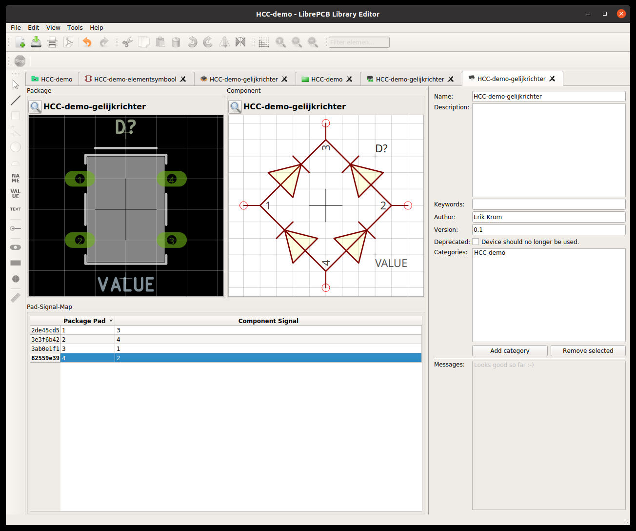 |
| Merge symbol and footprint into a part |
Finally
Here a number of important steps have now been treated for making a printing plate on the computer, including the drawing of your own electrical part. Not everything has been discussed, it is too much for that. Furthermore, this program is still fully developing and after writing this article a few updates have been released, so that some details have changed slightly. Feel free to view the manuals and documentation on libreppcb.org for current information and further deepening. A number of guidelines apply to designing your own electrical components, especially if you want to share your designs with others.